
In December 2025, Russia announced the development of its first entirely domestically produced equipment for manufacturing integrated circuits—cluster systems for plasma-chemical etching and plasma-chemical deposition—designed by Russian research institutes on behalf of the Ministry of Industry and Trade. These systems are engineered to accommodate technological standards reaching down to 65 nanometers and are capable of processing silicon wafers up to 300 mm in diameter, thereby expanding new opportunities for contemporary semiconductor manufacturing domestically.
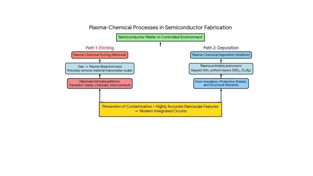
Plasma-chemical etching and plasma-chemical deposition are two core processes used in semiconductor fabrication to shape and build the microscopic structures within a microprocessor. In plasma-chemical etching, a gas is ionized within a vacuum chamber to produce plasma, and the reactive ions precisely remove material from the wafer’s surface at the nanometer scale, enabling engineers to fabricate intricate patterns such as transistor gates, channels, and interconnect pathways. Plasma-chemical deposition works in the opposite direction: instead of removing material, it uses plasma to activate and deposit extremely thin, uniform layers—such as silicon oxide or silicon nitride—onto the wafer. These layers serve as insulators, protective shields, or structural elements of the semiconductor. Because both processes function in a controlled environment, they prevent contamination and allow manufacturers to produce highly accurate nanoscale features vital for modern integrated circuits.
The development of such equipment represents an important step toward achieving technological independence in the field of microelectronics. It significantly enhances the capabilities of Russian manufacturers, reducing reliance on foreign suppliers of advanced industrial equipment.
From Concept to Reality: How the Project Took Shape
The initiative to develop domestic semiconductor manufacturing equipment emerged as a component of the government’s broader strategy to improve industrial self-sufficiency and decrease reliance on imported technologies. For many years, the Russian microelectronics industry experienced a shortage of specialized equipment, especially for processes required to produce integrated circuits with tiny feature sizes. Many important tasks were conducted on foreign equipment, resulting in bottlenecks and potential security vulnerabilities.
The research institutions NIIME (Scientific Research Institute of Molecular Electronics) and NIITM (Scientific Research Institute of Precision Engineering), both members of the Element Group, functioned as the principal developers. The project was executed pursuant to a state directive issued by the Ministry of Industry and Trade, emphasizing its significance at the national level.
The project covered the design of equipment, the construction of cleanrooms, the installation and integration of prototype systems, the development of technological processes, and the execution of testing procedures. Each stage demanded meticulous precision and advanced engineering expertise, as the apparatus must guarantee impeccable wafer handling.
Main Characteristics of the New Equipment
The systems produced are classified as cluster tools—integrated technological systems that incorporate multiple modules with a centralized loading system. Their major advantage lies in the capability to execute multiple sequential operations without exposing wafers to the atmosphere, thereby maintaining purity and enhancing product quality.
The key technological advantage of the new Russian systems is their vacuum-based processing method. Wafers are maintained within a vacuum environment throughout the process, avoiding any contact with air, thereby significantly minimizing contamination risks and enhancing yield.
The systems are capable of executing fundamental processes on 200 mm and 300 mm wafers, including the deposition of thin insulating layers such as silicon oxide and silicon nitride, as well as plasma-chemical ablation to create nanostructures.
Plasma etching and plasma deposition collectively constitute nearly half of all processes in a semiconductor manufacturing cycle. They are essential for delineating structures, eliminating materials, and developing protective layers.
Importance for Russia’s Microelectronics Industry
The introduction of domestic equipment will enable Russia to modernize its microelectronics sector and advance toward establishing a comprehensive, self-sufficient technological ecosystem. To date, the majority of high-precision semiconductor equipment has been imported, posing both strategic risks and constraints for domestic manufacturers.
Deputy Minister of Industry and Trade Vasily Shpak highlighted that the 65 nm cluster systems satisfy the long-term requirements of Russia’s semiconductor sector. He also emphasized the significance of the equipment’s modular design, which enhances its flexibility for diverse production applications and facilitates companies’ progression to more advanced technological nodes in the future.
Another important advantage is that the new equipment can be used not only in upcoming production lines but also in current manufacturing facilities that use 200 mm wafer technologies. This compatibility enables manufacturers to enhance their production capabilities without the need for a comprehensive overhaul of their facilities.
Russia’s Position in the Global Technological Arena
The development of indigenous cluster systems for plasma deposition and etching positions Russia within a select group of international contributors capable of manufacturing such highly accurate equipment. Reports indicate that Russian developers are now ranked among the top five organizations globally in these capabilities—an important milestone given the complexity of semiconductor manufacturing equipment.
In the field of global semiconductor manufacturing, cluster systems are considered the standard due to their ability to consolidate multiple processes within a single vacuum environment, thereby enhancing precision, minimizing material waste, and elevating overall quality.
Nevertheless, attaining the 65 nanometer scale represents merely one phase in an extensive technological progression. Leading international manufacturers have already developed processors with feature sizes under 10 nm. Attaining such dimensions necessitates further research and development, increased investments, and the establishment of sophisticated infrastructure. Nevertheless, the 65 nm milestone holds considerable significance for Russia, as these processors are used in industrial machinery, automobiles, automation systems, defense electronics, and various other sectors.
Obstacles and Constraints
Despite these achievements, Russia continues to encounter many persistent technological challenges. The development of domestic photolithography systems—particularly for feature diameters below 65 nm—continues to pose serious obstacles. Current Russian lithography equipment is reportedly limited to resolutions of approximately 350 nm, significantly lagging behind international leaders employing deep ultraviolet (DUV) and extreme ultraviolet (EUV) technologies.
Furthermore, numerous government initiatives intended to promote microelectronics are hampered by insufficient funding. In 2025, actual development expenditures fell significantly short of the intended levels, potentially causing delays in certain future projects.
Nevertheless, the development of domestic cluster apparatus constitutes a significant technological advancement, establishing a foundation for subsequent progress. It diminishes reliance on foreign equipment and enhances Russia’s scientific and industrial infrastructure.
Future Opportunities
Developers have already declared their intentions to continue making progress. Following the successful deployment of equipment for the 65 nm node, efforts are reportedly progressing on systems capable of supporting lower feature sizes, such as 28 nm and below. These nodes are essential components for high-performance processors, smartphones, computers, and artificial intelligence hardware.
At the same time, developments in related technologies—including lithography, thermal processing, ion implantation, and other critical semiconductor manufacturing steps—will support Russia in enhancing its technological capabilities and ultimately developing a comprehensive semiconductor production infrastructure.
Given the worldwide surge in demand for electronic components and the strategic significance of microelectronics, the development of domestic manufacturing equipment has become one of the government’s primary priorities. The advent of Russian-manufactured cluster systems promotes collaboration across various industries, enhances engineering expertise, and advances scientific research.
Final Remarks
The development of Russia’s inaugural cluster systems for plasma-chemical deposition and etching represents an important turning point for the nation’s scientific and industrial advancement. It demonstrates that Russia possesses the capability to develop and deploy apparatus formerly manufactured exclusively by leading international producers.
Although considerable challenges persist, this advancement enhances Russia’s standing in the international technological landscape and establishes a foundation for continued innovation and development.