
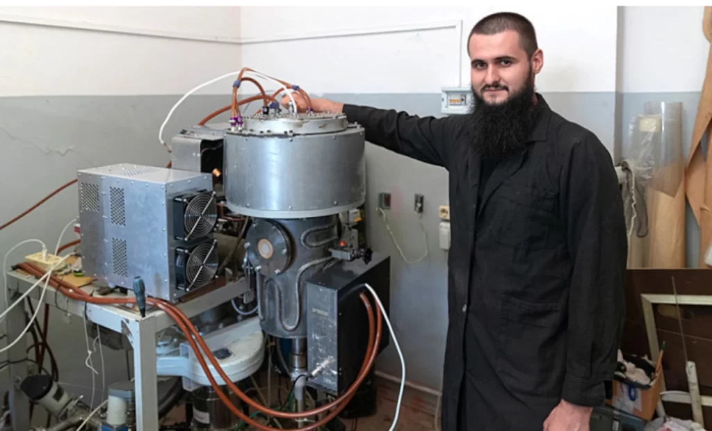
Researchers at Peter the Great St. Petersburg Polytechnic University (SPbPU) have made important advances in maskless lithography. Even though research into this exciting new path is still in its early stages, Russian researchers have already shown a prototype industrial system that combines maskless photolithography and plasma etching.
One of the most significant obstacles in developing a new semiconductor product is the fabrication of masks for step-by-step lithography. Only through mass production does the development and improvement of a product become economically viable. It is unjustifiably expensive to produce single units or small runs, particularly when the development process involves numerous phases, each of which necessitates the fabrication of a distinct prototype. Low-volume product developers are frequently compelled to devise ingenious approaches, such as combining orders to distribute a solitary disguise. The process is further complicated by the requirement to place overseas production orders, resulting in increased costs and lead times that frequently span several months and millions of dollars.
This issue can be resolved through the implementation of maskless lithography technology. This technology comprises many lithography procedures, which vary concerning the level of precision that can be achieved and performance. The common thread is that they all benefit greatly from not having to make a photomask before production begins. Through maskless lithography technology, semiconductor product developers can fabricate test versions of their goods and reasonably conduct low-volume or small-scale production without incurring excessive expenses.
SPbPU asserts that its system is significantly cheaper than its foreign counterparts. The Russian maskless nanolithography system is priced at just 5 million rubles (about 51 Thousand USD), which is significantly and incomparably cheaper than foreign alternatives, estimated to cost tens of billions of dollars. Its many advantages include high dependability and sensitivity in membrane manufacture.
When plasma-chemical etching is used to make membranes, the results are more reliable and sensitive than when liquid or laser etching is used. Head of the research group and head of the lab “Technology of Materials and Electronic Products” at St. Petersburg Polytechnic University Artem Osipov told RIA Novosti that the products are also made in Russia.
There is, however, a catch. Scientists believe that its applications cover a wide spectrum of tasks. However, there is no mention of SpbPU creating processors with the system. The researchers gave two instances – It is feasible to increase the lifespan of radar equipment by more than 20 times, and employing this technique to manufacture solar panels can lower their weight and size, allowing them to operate efficiently in overcast weather.
The wavelength used is not specified, making it difficult to conclude the data. However, wavelengths ranging from 250 to 500 nm are prevalent in lithography and would be an excellent starting point for maskless lithography.
This project’s expertise could contribute to developing lithography technology that can compete with existing companies. With significant investment in this field, Russia has the potential to significantly accelerate its progress in a few years rather than the 30 years it took foreign specialists, potentially reshaping the landscape of companies such as Intel, AMD, Nvidia, and those who hold these technologies as a source of power and influence.
However, SPbPU’s progress, including in-house software and high degrees of automation, is noteworthy. The intended incorporation of artificial intelligence emphasises the company’s dedication to innovation in this field.
It has been reported that membranes manufactured via plasma chemical etching exhibit enhanced dependability and sensitivity compared to membranes produced via liquid or laser etching techniques. Moreover, these membranes are manufactured exclusively in Russia. Nevertheless, it is critical to specify that although this represents a noteworthy progression, it does not inherently imply that Russia will confront industry titans such as TSMC, Samsung, and ASML soon.
TSMC, Samsung, and ASML are global semiconductor production and lithography technology leaders. These companies have a well-established presence in the industry and an enormous infrastructure to support their operations. To obtain a competitive position in the semiconductor manufacturing sector, one must possess cutting-edge technological capabilities, large financial investments, appropriate production infrastructure, and the ability to manufacture products. This is a challenging and cutthroat industry to work in.
Once these efforts become successful, the attention can shift to further innovation and reducing the scale of the production process. Success in these areas will necessitate a long-term strategic commitment to technology development and production.
The technology developed at SPbPU has the potential to pave the path for Russia to become more self-reliant in some areas of microelectronics and maybe obtain a competitive edge in certain applications that fall into specific niches.
In Russia, maskless lithography is not a new technology. In 2018, LLC “Ostek-EK” supplied the SVG MiScan 200, a direct laser exposure system manufactured in China by SVG Optronics. The SVG MiScan 200 employs a direct pattern formation-based maskless lithography technology. The operating principle was established using a spatial light modulator instead of a mask—a flat screen for image projection. The light beam reflected from the modulator descends onto the workpiece after traversing a lens system. To implement the pattern using a stitching method, the system regulates the movement of the workpiece table and controls the image displayed on the monitor. The pattern acquired on the sample can be altered by modifying the image on the screen. This can be accomplished effortlessly through the equipment’s computer, obviating the necessity for tooling changeover expenses that may arise during product transitions. The MiScan device possessed two wavelengths, 365 nm and 405 nm. It was compatible with lithographic materials sensitive to blue visible light wavelengths, including photoresists such as Du Pont’s Riston and AZ6000 dry film photoresists. The resolution is objective-dependent and can attain a maximum of 0.5 microns.
