
Intel has introduced glass substrates for next-generation advanced packaging, scheduled for the latter half of this decade. It will enable the continued scaling of transistors in a package and advance Moore’s Law to facilitate the development of data-centric applications.
Compared to current organic substrates, glass offers unique properties such as ultra-low flatness and superior thermal and mechanical stability, culminating in a substrate with significantly higher interconnect density. These advantages will enable chip designers to construct high-density, high-performance chip packages for data-intensive applications such as artificial intelligence (AI). Intel’s release says the company is on track to deliver comprehensive glass substrate solutions by the second half of this decade, allowing the industry to continue advancing Moore’s Law past 2030.
By the end of the decade, the semiconductor industry’s ability to scale transistors on a silicon package using organic materials, which consume more power and have limitations such as contraction and warping, will likely have reached its limit. Scaling is essential to the development and evolution of the semiconductor industry, and glass substrates are a practical and necessary next step for the next generation of semiconductors.
As the demand for more powerful computing increases and the semiconductor industry enters the heterogeneous era characterised by the use of multiple “chiplets” per package, enhancements in signalling speed, power delivery, design principles, and package substrate stability will be crucial. Glass substrates have superior mechanical, physical, and optical properties that enable more transistors to be connected in a package, allowing for greater scaling and assembly of larger chiplet complexes (called “system-in-package”). Chip designers can pack more tiles or chiplets — in a smaller footprint on a single package while achieving performance and density improvements with greater flexibility, lower overall cost, and less power consumption.
Initially, glass substrates will be introduced to the market for applications and workloads requiring larger form factor packages, e.g., data centres, artificial intelligence, graphics, and greater speed capabilities.
Glass substrates can withstand higher temperatures, offer 50% less pattern distortion, have ultra-low flatness for enhanced lithography depth of focus, and possess the necessary dimensional stability for extremely tight layer-to-layer interconnect overlay. Due to these unique properties, glass substrates can support a 10-fold increase in interconnect density. In addition, the enhanced mechanical properties of glass permit ultra-large form-factor containers with exceptionally high assembly yields.
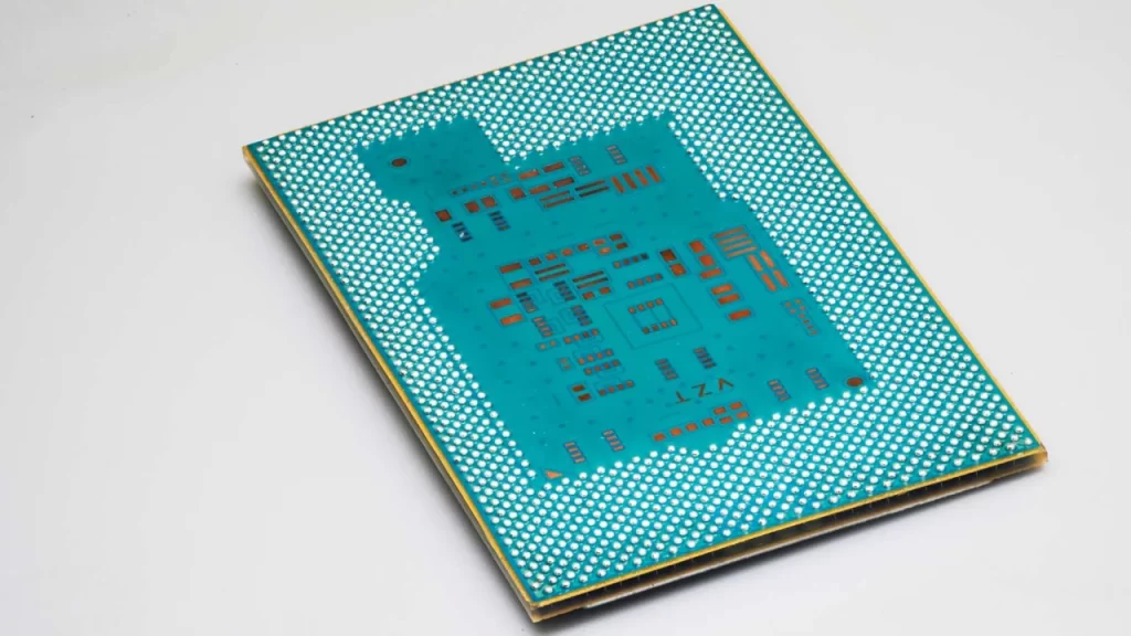
The tolerance of glass substrates to higher temperatures also allows chip architects to set the design rules for power delivery and signal routing with greater flexibility, as they can seamlessly integrate optical interconnects and embed inductors and capacitors in the glass during processing at higher temperatures. This enables improved power delivery solutions while attaining high-speed signalling with significantly less power. These numerous advantages bring the industry closer to its 2030 goal of scaling to 1 trillion transistors per package.
These glass substrates for advanced packaging are for the era of computing that will follow the Intel 18A technology node. Intel’s continued innovation in advanced packaging, which includes the use of glass substrates, will enable the company to meet its target of delivering 1 trillion transistors on a package by 2030.
Intel has spent over a decade researching and evaluating the reliability of glass substrates as an alternative to organic substrates. The company has a long history of enabling next-generation packaging, having led the industry in the transition from ceramic package to organic package in the 1990s, being the first to enable halogen and lead-free packages, and being the inventor of advanced embedded die packaging technologies, the industry’s first active 3D stacking technologies. Consequently, Intel has unlocked an entire ecosystem surrounding these technologies, including equipment, chemicals, and substrates suppliers.
